- 您现在的位置:买卖IC网 > Sheet目录537 > XR18W753IL48-F (Exar Corporation)IC RF TXRX 868-956MHZ 48QFN
�� �
�
�XR18W753�
�SINGLE� CHIP� 868MHZ� TO� 956MHZ� RF� TRANSCEIVER�
�2.0� PRODUCT� DESCRIPTION�
�REV.� 1.0.0�
�2.1�
�Radio� Frequency� Standards�
�The� XR18W753� is� designed� to� operate� in� licensed-free� European� 868� MHz� SRD,� North� American� /� Australian�
�915� MHz� ISM,� and� 950� -� 956� MHz� bands.�
�2.2�
�Transmitter� Block�
�The� transmitter� block� is� a� direct-up-conversion� I/Q� modulator� consisting� of� D/A� converters,� interpolation� filters,�
�balanced� I/Q� mixers� and� a� power� amplifier.�
�2.3�
�Receiver� Block�
�The� receiver� is� a� Low-IF� digital� receiver� consisting� of� a� low-noise� amplifier� (LNA),� I/Q� mixers,� IF� filters,� variable�
�gain� amplifiers,� and� A/D� converters.�
�2.4�
�Modem� Block�
�The� modem� block� is� a� Direct-Sequence-Spread-Spectrum� (DSSS)� O-QPSK� digital� modem� with� built-in�
�automatic� gain� control� (AGC),� Physical� Layer� Management� Entity� (PLME),� Frame� Check� Sum� (FCS)�
�computation,� and� Cyclical� Redundancy� Check� (CRC)� hardware.�
�2.5�
�Supporting� Block�
�The� supporting� block� in� the� XR18W753� includes� voltage/current� reference,� supply� voltage� stabilizer,� and�
�crystal� oscillator.�
�2.6�
�Baseband� Microcontroller� Interface�
�Interface� to� the� XR18W753� can� easily� be� made� via� the� I� 2� C� bus� as� in� the� XR18W750� baseband� microcontroller.�
�All� internal� registers� and� data� buffers� are� accessible� via� this� bus.� A� 16MHz� CMOS� clock� is� provided� to� the�
�microcontroller,� eliminating� the� cost� of� an� extra� clock� or� crystal.�
�2.6.1�
�I� 2� C-bus� Interface�
�The� I� 2� C-bus� interface� is� compliant� with� the� Standard-mode� and� Fast-mode� I� 2� C-bus� specifications.� The� I� 2� C-�
�bus� interface� consists� of� two� lines:� serial� data� (SDA)� and� serial� clock� (SCL).� In� the� Standard-mode,� the� serial�
�clock� and� serial� data� can� go� up� to� 100� kbps� and� in� the� Fast-mode,� the� serial� clock� and� serial� data� can� go� up� to�
�400� kbps.� The� first� byte� sent� by� an� I� 2� C-bus� master� contains� a� start� bit� (SDA� transition� from� HIGH� to� LOW�
�when� SCL� is� HIGH),� 7-bit� slave� address� and� whether� it� is� a� read� or� write� transaction.� The� next� byte� is� the� sub-�
�address� that� contains� the� address� of� the� register� to� access.� The� XR18W751� responds� to� each� write� with� an�
�acknowledge� (SDA� driven� LOW� by� XR18W751� for� one� clock� cycle� when� SCL� is� HIGH).� If� the� TX� FIFO� is� full,�
�the� XR18W751� will� respond� with� a� negative� acknowledge� (SDA� driven� HIGH� by� XR18W751� for� one� clock�
�cycle� when� SCL� is� HIGH)� when� the� CPU� tries� to� write� to� the� TX� FIFO.� The� last� byte� sent� by� an� I� 2� C-bus� master�
�is� a� stop� bit� (SDA� transition� from� LOW� to� HIGH� when� SCL� is� HIGH).� For� complete� details,� see� the� I� 2� C-bus�
�specifications.�
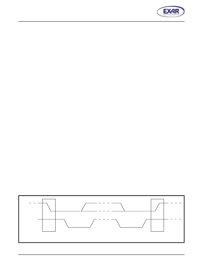
�F� IGURE� 5.� I� 2� C� S� TART� AND� S� TOP� C� ONDITIONS�
�SDA�
�SCL�
�S�
�START� condition�
�8�
�P�
�STOP� condition�
�发布紧急采购,3分钟左右您将得到回复。
相关PDF资料
XS-B14-CB2RB
SENSOR TEMP/HUM/LIGHT BATT XBEE
XT09-4II-RA-NA
MODEM RF 900MHZ RS232/485 NEMA 4
XT09-DK-MESH
KIT DEV 900MHZ W/MESH
XT09-MI
MODULE RF 900MHZ 1W 115K W/MMCX
XT09-PKI-EA-NA
MODEM RF 900MHZ 1W ETHER INT
XT09-SI
MODULE RF 900MHZ 1W 115K W/RPSMA
XU-A11
X-STICK 2.4GHZ USB TO XBEE
XV-8000CB :3 50.3000KHZ+/-60DPS
AUTOMOTIVE GYRO SENSOR +/-60DPS
相关代理商/技术参数
XR18W753L48-0A-EB
功能描述:界面开发工具 900MHz RF EVAL Board
RoHS:否 制造商:Bourns 产品:Evaluation Boards 类型:RS-485 工具用于评估:ADM3485E 接口类型:RS-485 工作电源电压:3.3 V
XR1901SN
制造商:Electro-Term/Hollingsworth 功能描述: 制造商:Electro-Term/Hollingsworth 功能描述:16-14awg No. 6 stud ring terminal - FAC STK
XR1902SN
制造商:HOLLINGSWORTH 功能描述:16-14awg No. 8 stud ring terminal - FAC STK
XR1903SN
制造商:HOLLINGSWORTH 功能描述:16-14awg No. 10 stud ring terminal - FAC STK - 1k in house
XR1906SN
制造商:HOLLINGSWORTH 功能描述:16-14awg 1/4 stud ring terminal - FAC STK
XR1906SNT
制造商:Electro-Term/Hollingsworth 功能描述:
XR1907S
制造商:Electro-Term/Hollingsworth 功能描述:
XR1907SN
制造商:HOLLINGSWORTH 功能描述:16-14awg 5/16 stud ring terminal - FAC STK